Pcb Panel Design Tool

Top Five Circuit Board Design Apps Pcb Design
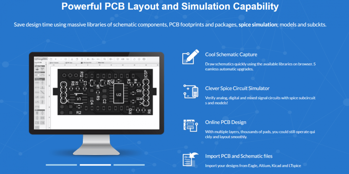
Build Pcb Online Using Web Based Eda Tools
Top Best Pcb Layout And Design Software For Macintosh

Pcb Design Procedures Pcb Design Schematic Design Tool Design
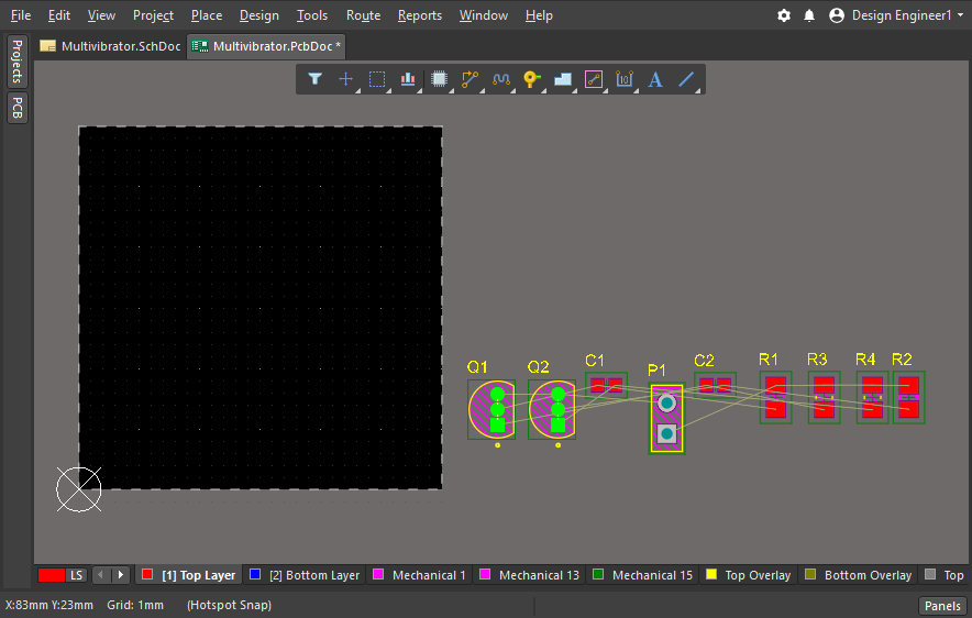
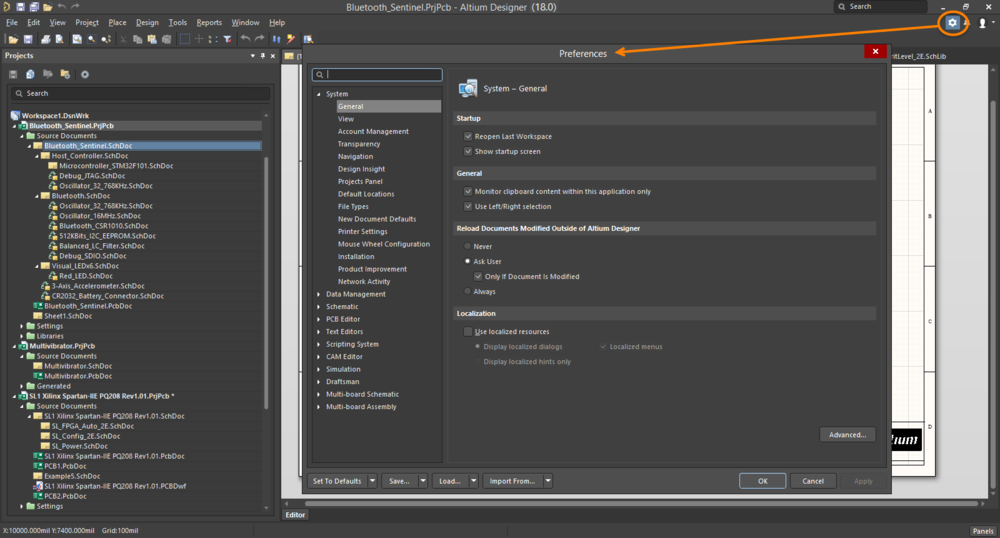
From Idea To Manufacture Driving A Pcb Design Through Altium Designer Altium Designer 18 0 User Manual Documentation

Make Hobbyist Pcbs With Professional Cad Tools By Modifying Quot Design Rules Quot 15 Steps With Pictures Instructables
Pcb panelization is one of the most essential modern tools we have when it comes to pcb manufacturing efficiency.
Pcb panel design tool. With the help of this tool simple labels can be created quickly and automatically. Design your panel with icape group software. With used step the design to be used can be selected. You can have a view of your panel with your personal pcb parameters.
Spatial resolution of 10 nanometers for precision. Osmond pcb is a pcb design software tool for electronics engineers using macs. Our panel design allowed you to create your electronic manufacturing document and successfully request the right quote. Developed with a highly intuitive style and use model orcad panel editor enables you to.
Swap top and bottom views by clicking on the bird s eye menu or using the tool menu icon. Orcad panel editor is a pcb assembly array panel design tool that intelligently automates the panel definition and documentation process to produce simple or complex pcb assembly panels in a fraction of the time versus traditional manual methods. Simply use our online pcb builder tool to upload gerber files review your board in a pcb viewer select a bid from a board house and follow the standard digi key checkout process. The pcbs are arranged according to their surrounding rectangles to save as much space as possible.
The pcb array introduces additional factors to consider like the number of parts on the array and how the parts are arranged on the array the. Depending on your design there may be other design considerations for the assembly process that should be considered. Panel name defines the name of the generated user. This guide focuses on array panelization to achieve the most parts per panel and the best pcb manufacturing price.
Use our free pcb panelizer tool below to determine how many pcbs will fit per panel. This pcb design tool gives users power and flexibility and eliminates artificial limits and restrictions to enable the design of boards of any size and shape and with as many layers as needed. Pcb panels not only make pc manufacturing more efficient reducing lead time but proper pcb panel use can resolve a lot of logistical problems including how to manufacture smaller printed circuit boards or boards with unusual shapes. Canvas and unit setting pcb tools layers and objects tool layer manager ratline pcb net board outline route tracks copper pour solid region design rule check footprint attributes design manager import changes panelize layout pcb without schematic pcb preview 3d model manager pcb information pcb modules generate fabrication file gerber export bom export pick and place file export dxf order pcb.
The size of the panel used for manufacturing which largely affects the price per board is mostly determined by the dimensions layer count and desired quantity of the pcbs.

Panelize A Round Pcb With Mouse Bites

Pcb Panelizer Gerber Tool Suite This Is Not Rocket Science

Free Pcb Design Tools Circuitmaker Pcb Design Pcb Design Software Tool Design

How To Do The Pcb Board Array Panelize
Design Panels Reference Altium Designer 20 2 User Manual Documentation
46 Top Pcb Design Software Tools For Electronics Engineers Pannam
Pads Pcb Design Tutorial Pcbcart

The Best Pcb Antenna Design Software Eases Antenna Implementation

Https Encrypted Tbn0 Gstatic Com Images Q Tbn 3aand9gcqlbnrpll06ikpt07z4vqizei5aqyqhsqf Xa Usqp Cau
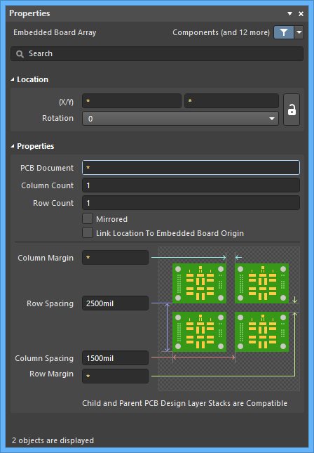
Embedded Board Array Altium Designer 20 2 User Manual Documentation
From Idea To Manufacture Driving A Pcb Design Through Altium Designer Altium Designer 19 0 User Manual Documentation
Activeroute Altium Designer 20 2 User Manual Documentation
10 Easy Steps To Design A Circuit Board Altium Designer

10 Free Pcb Design Software Pcb Design Software Pcb Design Software Design
Https Encrypted Tbn0 Gstatic Com Images Q Tbn 3aand9gcsos5hco9ycb2bz Lgbe9mqtfvnxtpz3kqfga Usqp Cau

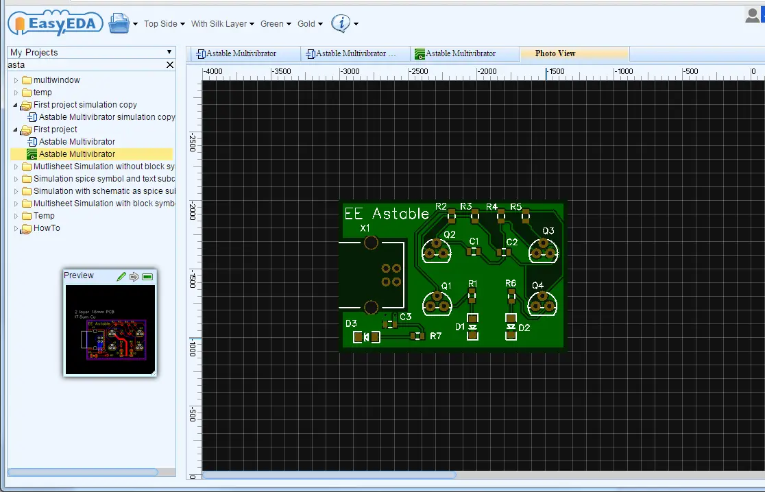
Forum Easyeda An Easier Electronic Circuit Design Experience Easyeda
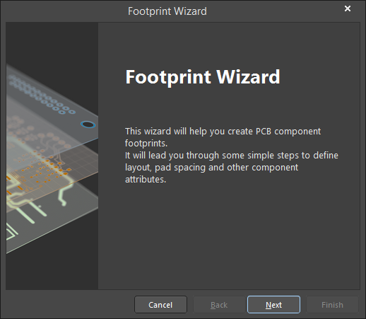
Creating The Pcb Footprint Altium Designer 20 2 User Manual Documentation

How To Make Panelized Pcb In Altium Designer

High Speed Pcb Design Circuit Board Design Pcb Layout Software
Circuit Board Builder Where Is Pcb Inspector In Altium 18
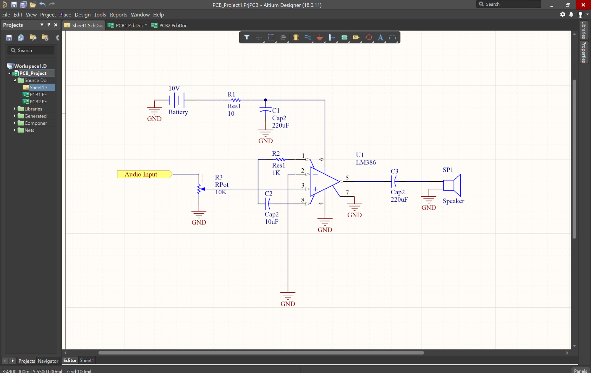
How To Create A Pcb Layout From A Schematic In Altium Designer Pcb Design Blog Altium

How To Export Eagle Pcb To Gerber Files Jlcpcb Help Support
An Introduction To Multi Board Design In Altium Designer Pcb Design Blog Altium Designer
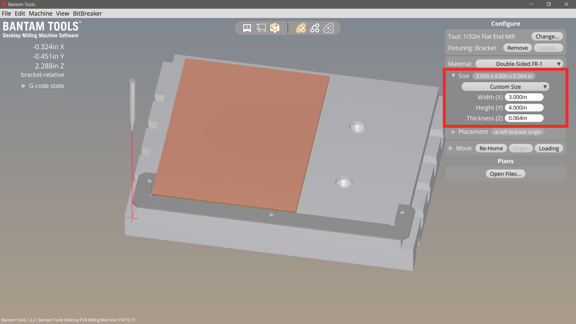
Double Sided Boards Bantam Tools

Pcb Layout Design In 2020 Layout Design Layout Pcb Design Software
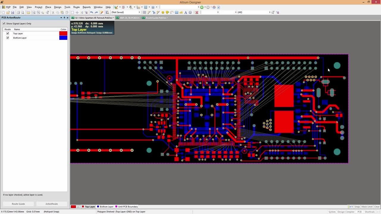
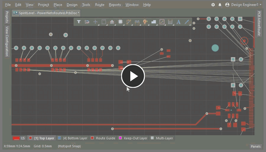
How To Route In Altium Designer 17 Using Activeroute Pcb Design Software Youtube

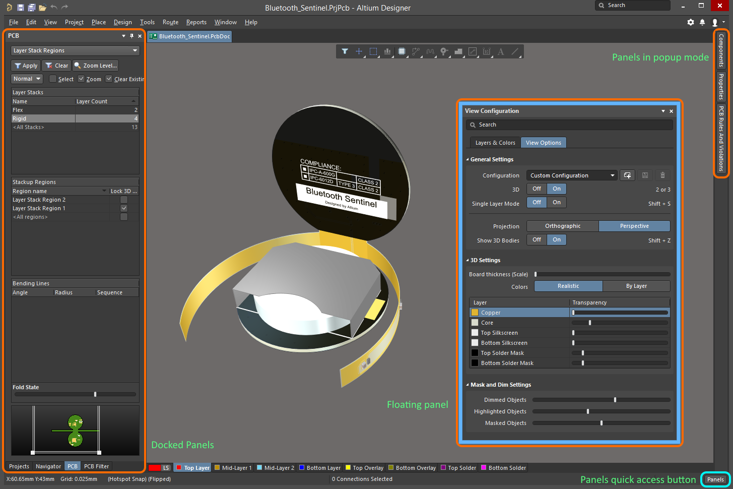
View Configuration Altium Designer 20 2 User Manual Documentation
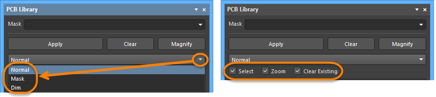
Pcb Library Altium Designer 20 2 User Manual Documentation

Pcb Design How To Create Circuit Boards Build Electronic Circuits Pcb Design Electronics Circuit Pcb Design Software

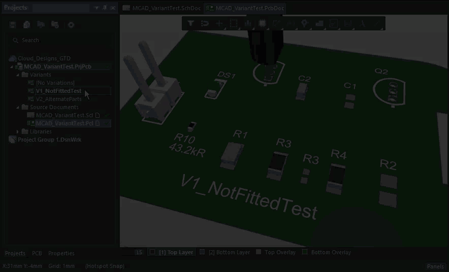
Ecad Mcad Codesign Altium Designer 19 0 User Manual Documentation
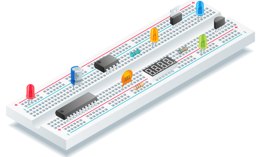
The Advantages Disadvantages Of Pcb Designing With Breadboards Altium Designer

Getting Started With Pcb Design Altium Com
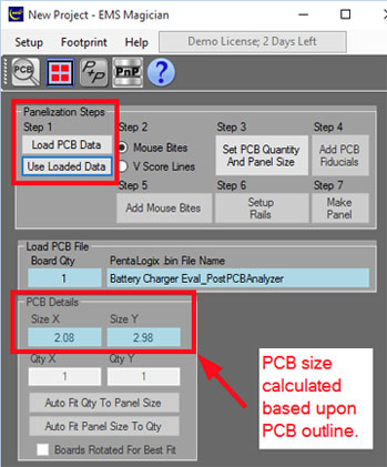
Single Design Panelizer Pentalogix Pentalogix

Pcb Layout Design Tool Circuit Simulator Layout Design Pcb Design

Printed Circuit Board Repair Tool Kits By Best Inc Circuit Board Printed Circuit Printed Circuit Board

Deciding On Pcb Design Tool As A Young Engineer

10 Free Pcb Design Software Pcb Design Software Pcb Design Circuit Board Design
How To Read A Pcb Assembly Drawing Pcb Design Blog Altium Designer

How To Choose The Best Pcb Design Software Pcb Design Pcb Design Software Electronics Design
Embedded Hardware Design And Development Services Integra Sources

Top 10 Free Pcb Design Software Con Immagini Elettronica Circuito

Pcb Antenna Design Simulation And Fabrication With Matlab Youtube

Electronic Circuit Board And Panel Design For Standard Enclosure

